More solar electrons with Aussie ingenuity
Solar panel manufacturing has nearly all left Australian shores. Phil Kreveld looks into a local innovation that could bring the technology back to home soil.
It doesn’t sound exciting when solar panels with thinner contact fingers are becoming a commercial reality, but it is; the new technology provides more available electrons per square centimetre than with current technology.
ADVERTISEMENT
More electrons and higher panel efficiency is a boon for solar system owners.
SunDrive, a Wollongong-based company with initial funding from the Australian Renewable Energy Agency (ARENA), has developed new techniques for attaching much narrower copper contact fingers than the existing practice which utilises relatively wide, silver-paste contacts. This is all part of the company’s product; high efficiency, thin layer, heterojunction (HJT) photovoltaic (PV) panels.
To get the business venture off the ground a funding round was led by the CSIRO’s venture capital outfit Main Sequence Ventures and the federally funded Clean Energy Finance Corporation (CEFC), with the latter confirming it had invested $7 million. Billionaire Mike Cannon-Brookes’ Grok Ventures and former prime minister, Malcolm Turnbull, are also involved. SunDrive chief executive, Vince Allan, studied under UNSW Professor Martin Green, who leads a team of researchers that have held solar cell efficiency research records for the past 30 years.
There’s definitely some weight behind the innovation.
SunDrive claims its metallisation process surpasses the patterning and copper metallisation quality and performance of other PV manufacturers. That being the case would constitute a major achievement considering that there has not been native PV manufacturing in Australia since 2010.
As Australia has very likely the world’s highest penetration of rooftop solar, SunDrive aims to concentrate its efforts in this market segment and its technological advantage augurs well for the company’s commercial success.
Replacing silver contact fingers with copper already presents a significant manufacturing cost reduction, copper being less than 1% the price of silver as well as being a thousand times more abundant. Furthermore, the cost of silver is rising and silver accounts for around 10% of the manufacturing price of a PV module.
However, Australia does not have the game to itself: researchers at the Fraunhofer Institute for Solar Energy Systems (ISE) in Freiburg, Germany, have taken on this challenge of substituting silver paste with copper. A team of researchers led by Dr. Markus Glatthaar, an expert in metallisation and structuring, has developed an electroplating process for the promising HJT technology and to replace silver with copper.
There is also a larger story: why are we not making our own solar panels? No good asking the Productivity Commission. They will go on about “economies of scale” and “comparative advantage” – all with respect to China, of course.
Economies of scale are a no-brainer, China has a gigantic advantage. As to comparative advantage, we have some very, very smart solar cell design and solid-state physics talent. China has a hold on growing monocrystalline silicon and that’s hard to match. However, getting the silicon wafers and designing new solar cells using locally invented epitaxial techniques, for example, HJTs, we can do that. It’s the story of SunDrive and hopefully, others who might want to emulate its example.
But there are there are things standing in the way of restarting local manufacturing: producing monocrystalline silicon wafers and their surface treatment. A lot of the technology was originated here. Dr. Zhengrong Shi, the one-time billionaire and SunDrive’s first ‘angel investor’ studied under Professor Green at UNSW but he heads the China-based SunTech, a significant world supplier of solar panels.
There’s no point in regretting past opportunities that slipped by, I could go on for a long time. The one that presents itself, and in particular to SunDrive, is the local manufacturer of high-efficiency panels for the Australian household, commercial and industrial rooftop market, the one that AEMO predicts will be delivering a third of 400 plus terawatt-hours of total annual energy by 2050.
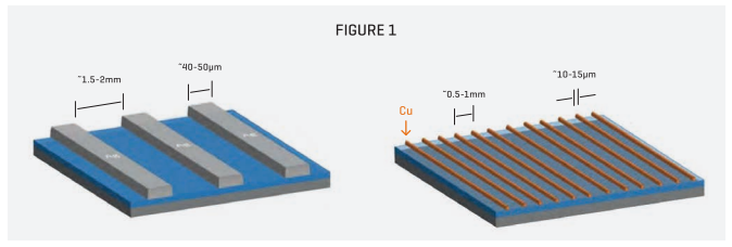
The copper contact fingers developed by SunDrive are much narrower than the silver-paste ones that are a standard feature of commercial panels. This is illustrated in Figure 1.
As is evident, there can be many more narrow copper fingers and the relative area ‘shadowed’ is of the same order as for silver, but the big advantage is that lateral loss of electrons is reduced thus adding to electron capturing efficiency. Although copper is substantially more cost-effective than silver, its application is not as straightforward as conventional screen printing with silver paste. The complexity of the process must be factored in, as each additional step adds to the overall cost.
SunDrive’s metallisation process incorporates high-accuracy lithography, with a resolution of less than ten micrometres and an improved adhesion of copper particles by a silver coating thus preventing oxidation of the copper. To ensure that the electrically conductive surface of the solar cell is not completely electroplated with copper, the areas of the surface that should not be coated must first be masked. The copper layer will only build up in the areas not coated with insulation. The contact fingers attach to the passive layer of the HJT photocell.
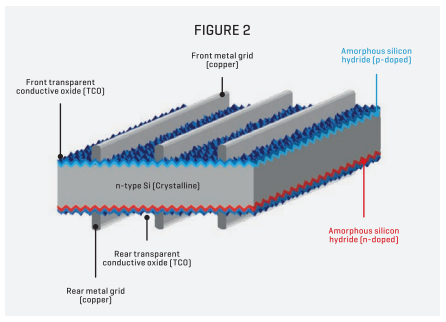
Figure 2 shows a typical HJT section of a photocell. Modern HJT solar cells have a low CO2 footprint on account of the low amounts of silicon used to produce them and when it comes to industrial protection, they achieve high levels of efficiency.
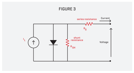
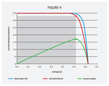
A transparent conductive oxide (TCO) film passivates the interface defects of crystalline silicon and doped amorphous silicon, resulting in high photoelectric conversion efficiencies. The narrow track copper contact fingers, shortens the distance for current transmission. This design minimises resistance, enhances current collection, and consequently improves the overall power generation efficiency. The top amorphous silicon layer is passivated to minimise defects present on the crystalline silicon surface. This is important because surfaces are dangerous discontinuities where electrons are lost to the external current path. Although it is a somewhat challengeable analogy, the shunt resistance in fig 3, representing the equivalent circuit of a solar cell, can be thought of as due to recombination processes preventing electrons from powering external circuits. That process reduces the effective current as supplied by the ideal current generator. Contact resistance, i.e. via the fingers, along with series resistance of the cell wiring reduces the maximum power point as shown in figure 4.
The effect is to shrink the I-V curve, from the open circuit voltage and therefore to shift the maximum power point voltage as well as to reduce the amount of maximum power available. Contact finger resistance plays a critical role in keeping the maximum power point as high as possible. The fill factor as shown by the shaded area is therefore the key efficiency indicator of a solar cell or panel.
In the HJT cell, the layer underneath the passivated one is doped amorphous silicon. To act as a solar cell, a PN junction must be formed with the bulk-doped substrate. Therefore, in a bulk N-doped cell, a P-layer must be introduced. The P-layer is thin compared to the bulk layer. The junction between the amorphous silicon and bulk silicon forms a depletion layer, effectively represented by the diode symbol in Figure 3. The P-layer can include an element such as boron, a trivalent metal. Silicon is tetravalent so inserting boron atoms in a silicon matrix means that an immediate silicon atom neighbour cannot pair one of its valence electrons, resulting in a net positive charge (a hole).
On the N-doped side, phosphorus atoms (that are pentavalent) have a valency shell electron to spare as the other four have paired with neighbouring silicon atoms, producing an excess of electrons in the conduction energy band and leaving the phosphorus atoms (lacking the electron donated for the conduction band) positively ionised.
Therefore, there is a net positive potential at the N side of the junction and a net negative potential on the P side, with acceptor atoms negatively ionised. The voltage resulting across the depletion layer is 0.6V between the P and N sides, or thereabouts. Of course, in the absence of an external circuit, the diffusing electrons eventually are cancelled by holes (electron bonding vacancies in the silicon crystal structure) as these are also present in the bulk material.
It is the depletion layer that, so to speak, powers the electrons created by photon interactions with the layers of the photocell. When photons hit the photocell, they can create more holes and electrons.
In the absence of a depletion layer, an external voltage would have to be applied to collect electrons and holes, i.e., cause a current to flow. The depletion layer is temperature-dependent so that as the ambient temperature rises, more and more electrons and holes are created on both sides of the P-N junction, and the region is said to become “intrinsic”, meaning that temperature-related production of electrons and holes (note: the electrons now originate from silicon valence shells, and therefore leave holes behind) overshadows the P and N dopants. This is the reason why solar panels lose efficiency with increasing temperature.
We are so comfortable with solar panels that the complexity of their interior functioning is not questioned. Yet their longevity and efficiency depend on those interior processes remaining unimpaired over the economic lifetime of a household’s or commercial enterprise’s investment. And that cannot be assumed.
Here again, there is room for Aussie ingenuity. Solar cells that are mass-produced today are very close to their efficiency limits. Limits are there to be broken and as to maximum efficiency, there is a long way to go as the sun with a surface temperature of 5,000°K, furnishes us a steady stream of photons. Thermodynamics indicates that with the Earth at a surface temperature of 300°K, maximum efficiency could be 94%. There’s a way to go.
-
ADVERTISEMENT
-
ADVERTISEMENT


