
Are bifacial solar panels worth it?
Solar panels are being installed at an incredible rate across the country. Phil Kreveld looks at some of the latest innovations on the technology side and how it works.
Janus was the Roman god of beginnings and endings. His bearded two-faced effigy presided over households, farming and all manner of daily activities in ancient days. However, two-faced Janus also reminds us of the duality of light – and electricity, in particular as that duality applies to bifacial solar panels. But before we get to that, how practical are bifacial solar panels for roof applications?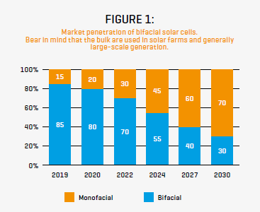
ADVERTISEMENT
Market penetration of bifacial solar cells. Bear in mind that the bulk are used in solar farms and generally large-scale generation.
They can make a difference, adding somewhere north of 5% relative to ‘unifacial’ solar panel installations. It can be higher but that would most probably require changes to rooves and physical layout.
Research conducted by the Australian National University (ANU) indicates that 20% more energy could be harvested from residential rooves through the use of bifacial solar panels than with standard panels. According to Marco Ernst from ANU, roof colour and surface treatment are important factors in determining reflectivity.
Professor Andrew Blakers at ANU developed ‘sliver’ bifacial technology, comprising a stack of laterally connected bifacial cells. It is a method for making thin, monocrystalline silicon solar cells that can capture sunlight from both sides.
Sliver cells are highly efficient, low cost and can be used to make flexible, transparent and lightweight solar modules. The technology was later transferred to Origin Energy which planned large-scale manufacturing for the Australian market by 2008, but finally, this never occurred due to price pressure from Chinese competition – a sad, and all too familiar story!
Ideally, bifacial panels are employed in solar farms where they can make use of albedo-reflected light. Albedo, Latin for ‘whiteness’, is the ratio of scattered reflected light to incident light (see Figure 2). As shown in the diagram, the albedo illumination, hitting the reverse side of the solar panel can be made use of to generate additional photovoltaic current thereby boosting effective panel efficiency. Scattered light from other than white surfaces, for example, grass, might be anywhere from 10% to 40% of direct illumination intensity. Generally, the appreciable albedo effect provides the ideal application for bifacial panels.
In Figure 3, essential bifacial construction features are shown, the bifacial panel utilising spaced ohmic contact fingers so that light can penetrate the rear surface. The rear surface is also glass-covered, adding to weight and manufacturing cost. The chart below provides information on the ‘front’ and rear-facing energy conversion efficiencies.
The ‘bifaciality factor’ (i.e., the ratio of direct rear to direct front illumination conversion efficiencies) is determined by the use of standard sun illumination of 1,000W/m². The difference in efficiencies is due in part to the location of the ‘depletion layer’ which can only be close to one surface in order to maximise light-to-electrical current conversion efficiency. This is discussed in more detail further down.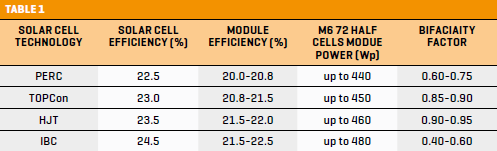
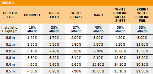
The albedo reflection is a rather variable factor in practice. The tabulation below provides diffuse reflection to direct light intensity ratios for a range of surfaces, the top line indicating the maximum reflectance, followed by its reduction as a function of panel height above the reflecting surface.
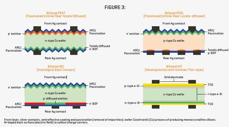
Front layer, silver contacts, antireflective coating and passivation (removal of impurities); wafer Czochralski (Cz) process of producing monocrystalline silicon; N+doped back surface (electric field) to collect charge carriers.
The tabulation entry for bright white roofing foil indicates a large albedo reflection. However, don’t get excited just yet, because the question of solar panel installation geometry and the duality of light (electromagnetic radiation/photon ‘particles’) plays an important role. In Figure 2, the ground affected may strike the rear surface of the panel with increasingly more oblique angles, thus reducing their absorption.
That brings in the laws of Fresnel, an 18th-century French physicist. They set out the reflection and transmission of light, quantitively. Absorption decreases as the angle of incidence increases. It is the transmitted light that is important as—here is the duality—it has the photons needed to create electrons. The graphs show the transmittance and reflectance for two polarisations (the planes of the electric field vector), one perpendicular to the glass surface, on one in a plane parallel to the surface (sunlight is randomly polarised). As the angle of incidence (measured always with respect to the normal of the surface) increases, the transmitted light becomes a smaller fraction—fewer photons.
It’s evident that even with a lot ‘albedo’ light reaching the rear of the panel, photon-electron generation is impacted. The treatment of the glass with antireflective coatings and surface ruling can ameliorate this somewhat. Once direct sunlight or albedo reflected light is absorbed (i.e., the transmitted fraction of incident light) we are dealing with light as photons (‘light particles’). The energy of a photon, E, is calculated as where h is Planck’s constant, c is the speed of light (3 x 1,010m/s) and is the wavelength of the light (refer to the component table of wavelengths for sunlight). Doing the maths, makes a blue photon have an energy of 2.5 electron volts (eV), which is more than enough to prise and electron loose—although things have been simplified a bit. Just for the case of astounding numbers, the standard sun of 1,000W per square metre is a shower of 4,000 million million million photons every second.

Typically, the range of a photon in silicon is a micron, a millionth of a metre. The business end of the solar cell, i.e. the depletion layer comprising of opposite electrical charge is also of the order of one to two microns. The thickness of a bifacial silicon wafer is 50 to 100 microns and that signifies that photoelectrons have some distance to travel to get to the depletion layer if they are created at the rear face of the wafer because acceptor-donor doping is at the direct sun-facing side.
Of course, they are also quickly absorbed, and it’s the photoelectrons created at the rear end that have to diffuse to the depletion region. Many get lost on the way, one reason why the rear side is not as efficient in conversion of useful charge carriers (electrons and holes).
The formation of the depletion layer is achieved with acceptor dopants (boron) and donor dopants (phosphorus). Silicon is tetravalent so inserting boron atoms in a silicon matrix means that an immediate silicon atom neighbour cannot pair one of its valence electrons, resulting in a net positive charge (a hole).
On the N-doped side, phosphorus atoms that are pentavalent have a valency shell electron to spare as the other four have paired with neighbouring silicon atoms, producing an excess of electrons in the conduction energy band, and leaving the phosphorus atoms (lacking the electron donated for the conduction band) positively ionised. Therefore, there is a net positive potential at the N side of the junction and a net negative potential on the P side, with acceptor atoms negatively ionised. The voltage resulting across the depletion layer is 0.6V between the P and N side, or thereabouts.
The physics of bifacial operation has shown that improvements can be gained by having a ‘tandem’ depletion layer at the rear face of the silicon wafer.
Research and development work is being done and briefly described here. Much of it originated in Spain, including the development of NPP+ and PNP structures, the latter being in effect a transistor albeit without a ‘base terminal’. The P+ layer signifies a higher level of acceptor doping. In the seventies, mono facial cells were developed suitable also for bifacial operation. Thereafter experimentation with the abovementioned doping structures took place, an NPN version being labelled a transcell because of its semblance to a transistor. The beneficial effect was studied of reducing P-doping in the base (central layer), where reduction of voltage in the emitter junction (front P-N junction) was compensated by voltage increase in the rear junction, while at the same time enabling higher diffusion length of minority carriers (holes in N regions, electrons in P regions) increasing the current output under bifacial illumination.
So much for theory. As shown by market trends (Figure 1), bifacial panels are predicted to become dominant, However, for rooftop installation, the advantages are not nearly as clear-cut.
Nevertheless, bifacial panels can also offer economic advantages although in order to ‘harvest’ them the overall lifetime of the entire PV installation has to be taken into account. The important factors are:
- Roof material: rooves with a high reflectivity index. An example would be light-coloured Colorbond roofing on a mounting angle.
- Avoidance of flush mounting: Shadowing cannot be avoided, obviously, but even with shadowing, albedo scattered light can make it to the rear surface of solar panels.
- Half panel, portrait orientation: this allows for the best overall performance, see Figure 4. As is obvious from the illustration, the reverse side of the panels is anything but uniformly illuminated.
To use as much albedo light as possible, solar panels should not be butted against each other but that requires taking up more roof real estate proportionately to standard panels. The obvious question begged then is why, given adequate real estate, one wouldn’t use that for extra standard panels?
Notwithstanding the set-up as pictured in Figure 6, in any practical installation of series/parallel connection of panels and a single maximum power point tracker, the benefit of bifacial panels may well be lost.
Therefore, it may be possible to use microinverters for use with small groups of panels. It appears that for domestic and commercial applications, a carefully considered design approach is recommended. For example, bifacial panels as curtains in an east-west orientation, structurally covered by a transparent roof.
If combined with standard panels, separate maximum power point trackers and inverters would be advisable.
All in all, given the current state of the art, the choice between standard and bifacial panels would appear to be one of price only for average suburban locations. On the other hand, in regional areas, where energy independence may be more critically important, bifacial panels in curtain applications, or as elevated applications on rooves may make good economic sense.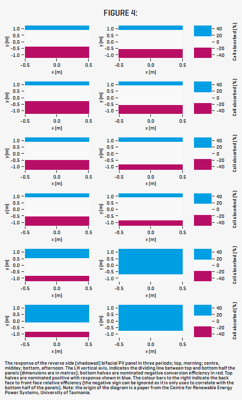
-
ADVERTISEMENT
-
ADVERTISEMENT
