What’s the difference between P and N-type solar panels?
The modern solar panel industry is focused on N-type solar panels over P-doped panels but little is really known about the two types that grace Australian roofs. Phil Kreveld explains.
N-doped solar panels are becoming the popular solution in the industry, often preferred over P-doped panels. Despite this, there are only small performance differences between the two and both are either monocrystalline or polycrystalline, so why are N-doped panels the go-to option?
ADVERTISEMENT
It’s important that solar installers understand the differences between the two, wrapping their heads around the physics of the two to help deliver the best possible outcome in a solar investment.
Firstly, what are P and N dopants?
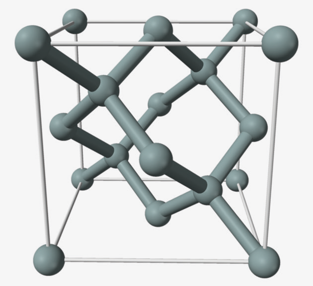
The base material of solar panels is silicon and in its crystalline form, silicon atoms are arranged in a diamond lattice.

DIAGRAM 1: Silicon has the diamond cubic crystal structure with a lattice parameter of 0.543nm. The nearest neighbour distance is 0.235nm
The atomic number of silicon in the periodic table of elements is 14. There are 14 protons of positive charge, e+ (1.6 x 10⁻¹⁹ coulombs), and the same number of negative charge electrons, with four in the outer (valence) ring.
It’s the valence ring electrons that provide the bonds with neighbouring silicon atoms to form crystal structures by sharing their valence electrons.
Silicon is a class IV element (four electrons available for bonding) and phosphorus (P, its element symbol) is a class V element with five valence electrons. It can be used as a bulk dopant in silicon, in low concentrations, capable of donating one of its valence electrons for the conduction of electricity.
Being an electron donor makes phosphorus an N dopant. This is a little confusing because we now turn our attention to P dopants, of which boron (element symbol B) is the element of interest. Boron is a class III element with three valence electrons, therefore, when it is a part of a silicon crystal array, it creates an electric charge vacancy, in effect a net positive charge of one e+ (this is referred to as a ‘hole’ but is every bit as much of a charge carrier as an electron).
A mechanical analogue is a line of traffic, bumper to bumper—when one car is removed, the following cars move up in sequence. Viewed from above, the one-car vacancy moves towards the end of the line of traffic. In an electric field, holes will drift in the opposite direction to electrons and the total current is the sum of both charge carriers.
P dopants like boron, contribute positive minority charge carriers while N dopants like phosphorus contribute negative minority carriers.
Pure silicon is an insulator, although it can easily be made a semiconductor by means of dopants. The main characteristic of semiconductors is their Fermi level, which is the maximum energy a valence electron can have at absolute zero (-273°C), halfway between its energy in the valence shell and the energy in the conduction band.
As the temperature is increased from absolute zero, some valence electrons have sufficient thermal energy to be raised to the conduction band, leaving ionised silicon atoms at the valence level. Overall, there is of course charge neutrality as an equal number of electrons and ionised (positively charged) silicon atoms are created.
For a semiconductor to act as a solar cell a PN junction must be formed in the bulk-doped substrate. Therefore, in a bulk N-doped cell, a P-layer must be introduced. The P-layer is thin compared to the bulk layer.
This is the reverse of the situation for most solar cells which have a thin N-layer in a bulk P-substrate. The majority of current carriers in the P-substrate cells are electrons and for the N-substrate cells the majority of carriers are holes.
Another way of visualising holes is the process of ionisation of P-dopants, transferring from one atom to the next and so on. At the rear contact of a cell, holes are neutralised by electrons, therefore contributing to electric current.
The thin-bulk layer interface becomes part of the so-called depletion layer. In the case of N solar cells, the boron dopant is present in much higher concentrations than the bulk N dopant. The P-layer is positively charged, electrons having diffused throughout the semiconductor (note: there is as yet, no external circuit).

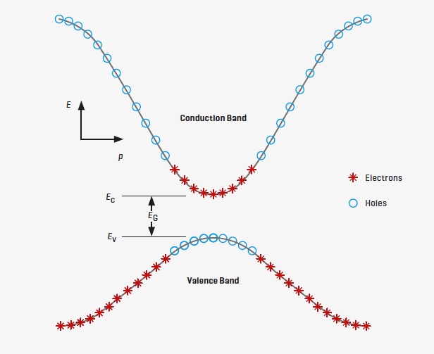
The diagram of a semiconductor shows the lower energy valence electron level
(Ev) and conduction electron level (Ec). The Fermi level is halfway between
the conduction and valence levels. Valence electrons within a certain range of
momentum (p) can readily transition to the conduction level as temperature
increases. When light photons impinge on the semiconductor, their energy can lift
valence electrons into the conduction band.
The voltage resulting across the depletion layer is 0.6V, or thereabouts. Of course, in the absence of an external circuit, the diffusing electrons eventually are cancelled by holes as these are also present in the bulk material.
As discussed in previous articles, the solar cell can be thought of as a current generator with a diode in parallel, formed by the depletion layer. Without an external circuit, the cancellation of charge carriers is in effect, taking place in the diode. Inspection of the diode current versus voltage characteristic shows a very high resistance (slope of the voltage) until about 0.6V. If a resistance of a much lower value is placed across the cell, charge carriers can flow through the external circuit—and provide power.
The choice therefore of fabrication methods that can increase the forward voltage of the depletion layer diode increases the range of resistive load that can be attached as well as increasing the maximum power point.
Theory is one thing, practice is another: producing pure grades of silicon from metallurgical grade silicon divides into polycrystalline and monocrystalline wafers. The polycrystalline wafers are produced from a casting process and the monocrystalline wafers use a process called the Czochralski process after the Polish scientist, Jan Czochralski.
As already mentioned, monocrystalline panels might have intrinsically higher efficiency than the poly-form which has many lattice faults that interfere with the production of charge carriers of sufficient range to allow their collection at the cell’s terminals.
For example, silicon is not a direct bandgap material in which the conduction band mirrors the valence band. Energy by way of lattice vibration is required to lift valence electrons to the conduction band. Crystal lattice vibration is a function of temperature and is in part dependent on the crystal structure.
Light-induced degradation of photovoltaic cells is caused by boron-oxygen defects and has been found to affect silicon devices, whose performance depends on minority charge carrier diffusion lengths. The defects are a common limitation in Czochralski-grown P-type silicon, and their recombination activity develops under charge carrier injection and is, thus, commonly referred to as light-induced degradation.
In effect, the same defect can be found in polycrystalline cells but the severity is less because of reduced high-temperature exposure during fabrication as opposed to the Czochralski method. Solving light-induced degradation has attracted some expensive methods including the implantation of germanium and gallium. Over recent years, phosphorus has been used rather than boron which forms boron-oxygen dimers resulting in increased charge carrier trapping.
The claims being made for the superiority of P bulk dopant panels in the early lifetime of solar panels have to be weighed against other factors that can affect cell performance including sodium ion migration from glass and potential induced degradation (PID) due to the potential between the photovoltaic module and its earth structure.
With high voltage between the structure and the high-voltage layer deterioration via leakage current takes place. The electrons in the PV module material may escape through the soil structure and the resulting polarization affects the electrical performance of the PV cells.
In view of the various problems due to deficiencies in manufacturing, material degradation, hotspots shortening panel life, the question isn’t just about the theoretical advantages of N-doping versus P-doping.
At present, passivated emitter and rear contact (PERC) solar cells that use P-type wafers account for 82% of the global photovoltaic power market, and they are expected to account for at least 50% of the market until 2031.
It makes a lot of sense therefore to use the concept of levelised cost of electricity which has taken into account the energy conversion efficiency performance over the lifetime of the solar panel. On that basis disadvantages such as light-induced degradation, which is highest in the first months of operation, but then levels off, might well turn out of small consequence.
-
ADVERTISEMENT
-
ADVERTISEMENT


